Controlling spin current polarization through non-collinear antiferromagnetism
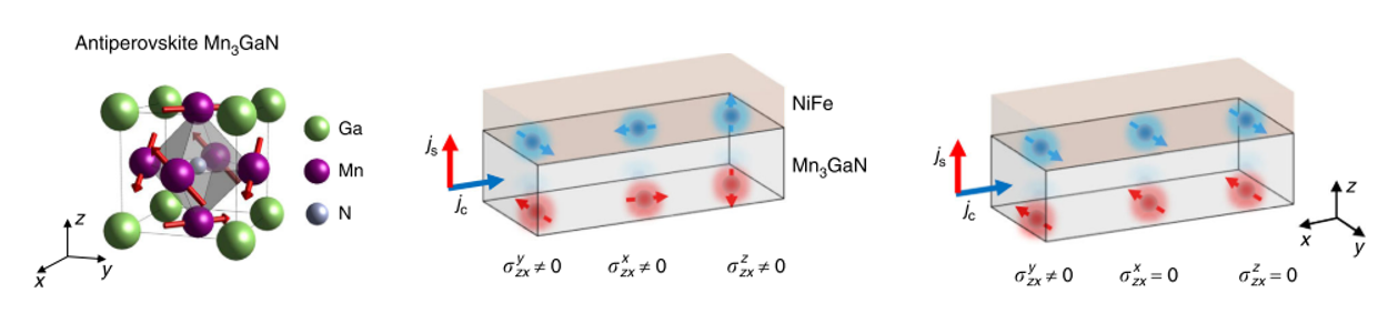
Mg3GaN unit cell with Mn spins (arrow) forming a Kagome-type lattice in the (111) plane. The Py/MGN bilayer's spin-Hall spin polarization is shown in the low and high symmetry states.
|
The interconversion of charge and spin currents via spin-Hall effect is essential for spintronics. Energy-efficient and deterministic switching of magnetization can be achieved when spin polarizations of these spin currents are collinear with the magnetization. However, symmetry conditions generally restrict spin polarizations to be orthogonal to both the charge and spin flows. Spin polarizations can deviate from such direction in nonmagnetic materials only when the crystalline symmetry is reduced. Here, we show control of the spin polarization direction by using a non-collinear antiferromagnet Mn3GaN, in which the triangular spin structure creates a low magnetic symmetry while maintaining a high crystalline symmetry. We demonstrate that epitaxial Mn3GaN/permalloy heterostructures can generate unconventional spin-orbit torques at room temperature corresponding to out-of-plane and Dresselhaus-like spin polarizations which are forbidden in any sample with two-fold rotational symmetry. Our results demonstrate an approach based on spin-structure design for controlling spin-orbit torque, enabling high-efficient antiferromagnetic spintronics.
Nan, T., et al. "Controlling spin current polarization through non-collinear antiferromagnetism." Nature communications 11.1 (2020): 1-7.
|
|
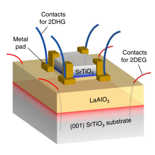
Two-dimensional hole gas at LaAlO3/SrTiO3 interface
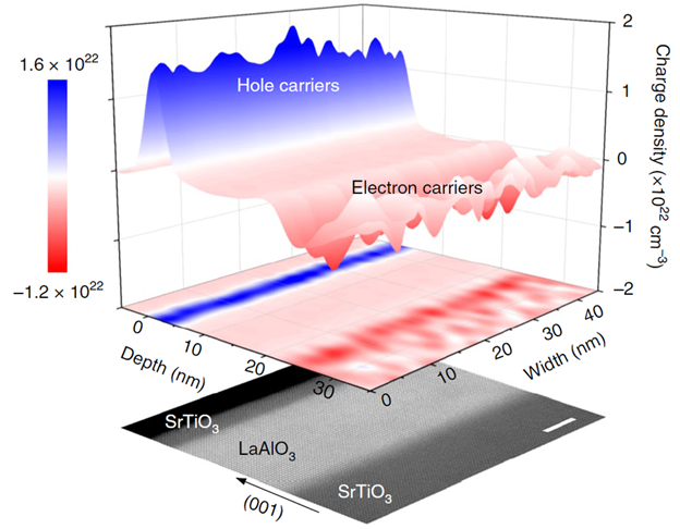
Charge distribution in the STO/LAO/STO heterostructure. (up) The charge-density map of the STO/LAO/STO heterostructure obtained by the in-line electron holography technique. The top and bottom interfaces clearly show the positive and negative charges, respectively. (down) The STEM–ADF image of the entire STO/LAO/STO heterostructure. Scale bar, 5 nm.
|
|
The discovery of a two-dimensional electron gas (2DEG) at the LaAlO3/SrTiO3 interface has resulted in the observation of many properties not present in conventional semiconductor heterostructures, and so become a focal point for device applications. Its counterpart, the two-dimensional hole gas (2DHG), is expected to complement the 2DEG. However, although the 2DEG has been widely observed, the 2DHG has proved elusive. Herein we demonstrate a highly mobile 2DHG in epitaxially grown SrTiO3/LaAlO3/SrTiO3 heterostructures. Using electrical transport measurements and in-line electron holography, we provide direct evidence of a 2DHG that coexists with a 2DEG at complementary heterointerfaces in the same structure. First-principles calculations, coherent Bragg rod analysis and depth-resolved cathodoluminescence spectroscopy consistently support our finding that to eliminate ionic point defects is key to realizing a 2DHG. The coexistence of a 2DEG and a 2DHG in a single oxide heterostructure provides a platform for the exciting physics of confined electron– hole systems and for developing applications.
Störmer, H. L., and W-T. Tsang. "Two-dimensional hole gas at a semiconductor heterojunction interface." Applied Physics Letters 36.8 (1980): 685-687.
Bark, C. W., et al. "Tailoring a two-dimensional electron gas at the LaAlO3/SrTiO3 (001) interface by epitaxial strain." Proceedings of the National Academy of Sciences 108.12 (2011): 4720-4724.
Podkaminer, J. P., et al. "Creation of a two-dimensional electron gas and conductivity switching of nanowires at the LaAlO3/SrTiO3 interface grown by 90o off-axis sputtering." Applied Physics Letters 103.7 (2013): 071604.
|
|
Epitaxial Thin Films of the Topological Crystalline Insulator Sr3SnO
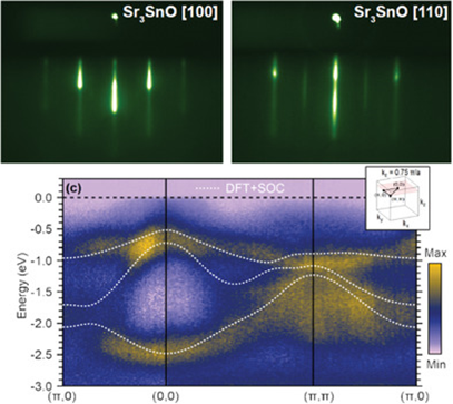
RHEED diffraction pattern of a Sr3SnO thin film along the [100] and [110] crystallographic directions. The band structure of Sr3SnO calculated by DFT and measured by ARPES. The agreement between the bulk theoretical calculations and the experiments suggest the TCI nature of Sr3SnO.
|
|
Topological materials are derived from the interplay between symmetry and topology. Recent advance in topological band theories has identified antiperovskite oxide Sr3SnO as a topological crystalline insulator, a new electronic phase of matter where the conductivity in its (001) crystallographic planes is protected by crystal point group symmetries. The realization of such material, however, is challenging. Guided by thermodynamic calculations, we designed a deposition approach to achieve the adsorption-controlled growth of epitaxial Sr3SnO single crystal films. In-situ transport and Angular Resolved Photoemission Spectroscopy analysis revealed the metallic and non-trivial topological nature of the as-grown samples. Compared with conventional deposition techniques, the synthesis route demonstrated in this work shows remarkable superiority in sample quality and is readily to be adapted for producing other topological systems with antiperovskite structures. The successful realization of thin films of topological crystalline insulators opens opportunities to manipulate topological states by tuning symmetries via epitaxial strain and heterostructuring.
Ma, Yanjun, et al. "Realization of epitaxial thin films of the topological crystalline insulator Sr3SnO." Advanced Materials 32.34 (2020): 2000809.
|
|
|
Superconducting Nb3Sn thin films for RF resonator applications
|
Superconducting radio-frequency (SRF) resonator cavities provide extremely high quality factors > 1010 at 1-2 GHz and 2K in large linear accelerators of high-energy particles. The maximum accelerating field of SRF cavities is limited by penetration of vortices into the superconductor. Present state-of-the-art Nb cavities can withstand up to 50 MV/m accelerating gradients and magnetic fields of 200-240 mT which destroy the low-dissipative Meissner state. Achieving higher accelerating gradients requires superconductors with higher thermodynamic critical fields, of which Nb3Sn has emerged as a leading material for the next generation accelerators. To overcome the problem of low vortex penetration field in Nb3Sn, it has been proposed to coat Nb cavities with thin film Nb3Sn multilayers with dielectric interlayers. Here, we report the growth and multi-technique characterization of stoichiometric Nb3Sn/Al2O3 multilayers with good superconducting and RF properties. We developed an adsorption-controlled growth process by co-sputtering Nb and Sn at high temperatures with a high overpressure of Sn. The cross-sectional scanning electron transmission microscope images show no interdiffusion between Al2O3 and Nb3Sn. Low-field RF measurements suggest that our multilayers have quality factor comparable with cavity-grade Nb at 4.2 K. These results provide a materials platform for the development and optimization of high-performance SIS multilayers which could overcome the intrinsic limits of the Nb cavity technology.
Vaswani, C., et al. "Terahertz second-harmonic generation from lightwave acceleration of symmetry-breaking nonlinear supercurrents." Physical Review Letters 124.20 (2020): 207003.
Yang, X., et al. "Terahertz-light quantum tuning of a metastable emergent phase hidden by superconductivity." Nature materials 17.7 (2018): 586-591.
|
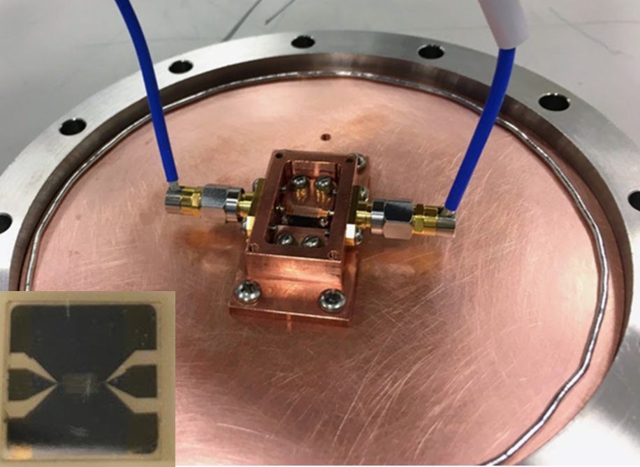
Patterned Nb3Sn thin films on Al2O3 to make a coplanar waveguide to determine figures of merit of Nb3Sn for use in RF superconducting resonators.
|
|
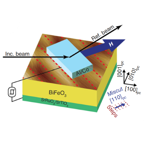
Strain engineering of multiferroic BiFeO3 thin films to induce monodomains
|
Multiferroic BiFeO3 has attracted great interest due to its promising application to magnetoelectric devices. Due to this low symmetry, eight possible polarization (ferroelectric) variants, which correspond to four structural (ferroelastic) domains, may form in the films, leading to complex domain patterns with both {100} and {101} twin boundaries. Such a complex domain structure can deteriorate the ferroelectric response of the system by external electric field, and complicates the examination of the coupling between magnetic and ferroelectric order parameters in BiFeO3. We have demonstrated the selection of domain structure variants in epitaxial BiFeO3 films and consequently significant improvement in ferroelectric switching behavior and leakage current by employing miscut in cubic (001) SrTiO3 substrates.
Price, N. Waterfield, et al. "Strain Engineering a Multiferroic Monodomain in Thin-Film Bi Fe O 3." Physical Review Applied 11.2 (2019): 024035.
Saenrang, Wittawat, et al. "Deterministic and robust room-temperature exchange coupling in monodomain multiferroic BiFeO 3 heterostructures." Nature communications 8.1 (2017): 1-8.
Price, N. Waterfield, et al. "Electrical Switching of Magnetic Polarity in a Multiferroic BiFeO 3 Device at Room Temperature." Physical Review Applied 8.1 (2017): 014033.
Zhao, T., et al. "Electrically controllable antiferromagnets: Nanoscale observation of coupling between antiferromagnetism and ferroelectricity in multiferroic BiFeO3." Nature Mater 5 (2006): 823-829.
|
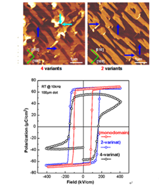
In-plane PFM images, P-E loops and leakage currents of of 4, 2 and 1 variant (001) BiFeO3 thin films.
|
|
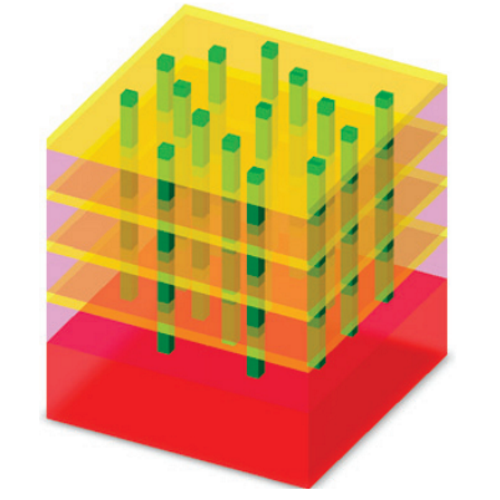
Charge density wave modulation in BaPbO3/BaBiBO3 Superlattices
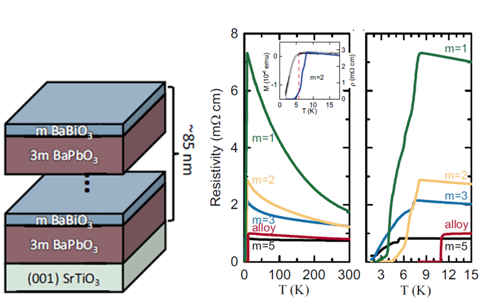
Schematic of BaBiO3, BaPbO3 superlattice structures. Full temperature range resistivity vs temperature. The inset of overlays the transition probed by resistive measurements (blue) with out-of-plane (black) and in-plane (gray) onset of diamagnetism (red dashed line) for m = 2. Transition region of superconducting samples.
|
|
Anisotropic spin-orbit torque generation in epitaxial SrIrO3 by symmetry design
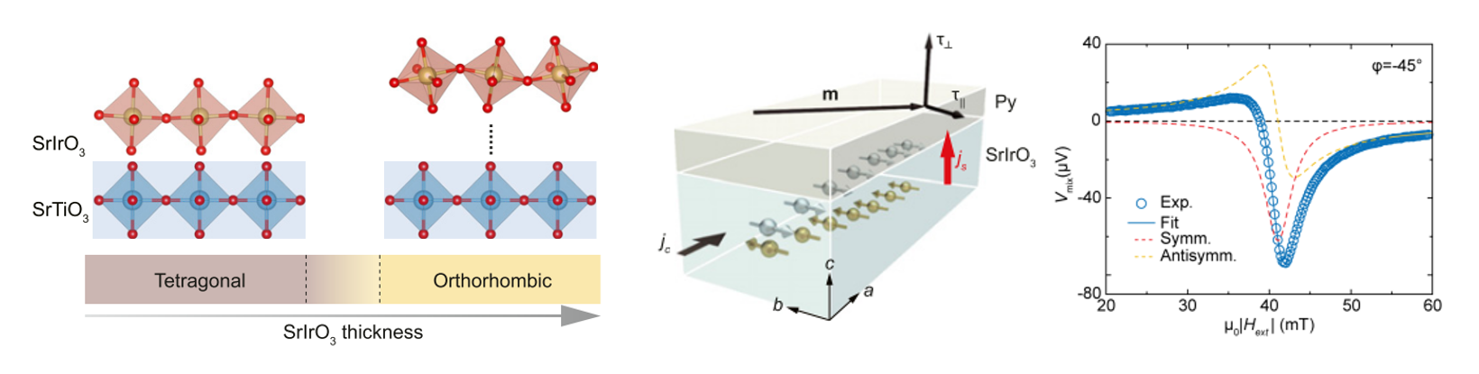
Schematic illustrations of the lattice symmetry of SrIrO3 when grown on cubic nontilted SrTiO3, where a partial suppression of the IrO6 octahedral tilt exists up to a certain thickness before a tilted octahedral pattern is established in thicker films. Schematic of the Py/SrIrO3 bilayer on SrTiO3(001) and the current-induced torque geometries. ST-FMR spectrum (fitted to a Lorentzian function, solid line) for a 3.5 nm Py/8 nm (20 uc) SrIrO3 sample (20 µm × 40 µm) with microwave current applied along the [110]o axis.
|
|
Modern spintronics operate based on the spin-to-charge interconversion, where charge current flowing through materials and interfaces with the strong spin-orbit interaction generates spin current via the spin-Hall effect. Here, we report the discovery of a class of intrinsic spin-Hall materials: 5d transition- metal complex oxides. In these materials, a delicate interplay between spin-orbit coupling and electron correlation exists, which can lead to nontrivial spin-related quantum transport phenomena. In particular, we find that epitaxial perovskite SrIrO3 thin films generate room-temperature spin currents via the spin-Hall effect more efficiently than those previously reported for elemental heavy metals. Furthermore, the efficiency can be modified by epitaxially tailoring the anisotropic SrIrO3 crystalline symmetry, thus demonstrating a path toward engineering efficient room-temperature spintronics.
Nan, Tianxiang, et al. "Anisotropic spin-orbit torque generation in epitaxial SrIrO3 by symmetry design." Proceedings of the National Academy of Sciences 116.33 (2019): 16186-16191.
|
Isostructural metal-insulator transition in VO2
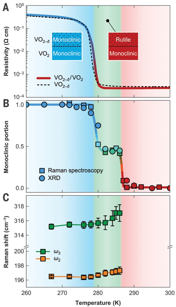
Electrical resistivity versus temperature of VO2−δ (8 nm)/VO2 (8 nm) bilayer (solid line) and 8-nm-thick VO2−δ single layer (black dashed line), measured upon cooling. Metallic and insulating phases are represented by red and blue colors, respectively. (B) Monoclinic portion as a function of temperature. (C) Temperature dependence of monoclinic Raman shift. Error bars denote SD of the fitted Raman peak position. We fit the measured Raman peak with a Gaussian curve.
|
|
The metal-insulator transition in correlated materials is usually coupled to a symmetry lowering structural phase transition. This coupling not only complicates the understanding of the basic mechanism of this phenomenon but also limits the speed and endurance of prospective electronic devices. We demonstrate an isostructural, purely electronically driven metal-insulator transition in epitaxial heterostructures of an archetypal correlated material, vanadium dioxide. A combination of thin-film synthesis, structural and electrical characterization, and theoretical modeling reveals that an interface interaction suppresses the electronic correlations without changing the crystal structure in this otherwise correlated insulator. This interaction stabilizes a nonequilibrium metallic phase and leads to an isostructural metal-insulator transition. This discovery will provide insights into phase transitions of correlated materials and may aid the design of device functionalities.
Lee, D. A. E. S. U., et al. "Isostructural metal-insulator transition in VO2." Science 362.6418 (2018): 1037-1040.
Briggs, Ryan M., Imogen M. Pryce, and Harry A. Atwater. "Compact silicon photonic waveguide modulator based on the vanadium dioxide metal-insulator phase transition." Optics express 18.11 (2010): 11192-11201.
Lee, Jaeseong, et al. "Epitaxial VO2 thin film-based radio-frequency switches with thermal activation." Applied Physics Letters 111.6 (2017): 063110.
|
|
Point defect control in SrTiO3 by metal-organic pulsed laser deposition
|
Point defects have played a major role in tuning the properties of materials over the last few decades. In quantum heterostructures based on complex oxides, however, the control of individual point defects continues to be challenging arising mostly from inherent non-stoichiometry. Herein, the ability to tune point defects in oxide-based quantum heterostructure LaAlO3/SrTiO3 (LAO/STO) is demonstrated using a newly-developed metal-organic pulsed laser deposition (MOPLD) technique. Density functional theory (DFT) calculations predict that increasing the ratio of [antisite Ti (TiSr)]/[strontium vacancies (VSr)] reduces the equilibrium amount of oxygen vacancies (VO) which is the most dominant scattering center at low temperatures. X-ray diffraction and Raman spectroscopy show that the MOPLD technique, with titanium tetraisopropoxide (TTIP) used as Ti source, provides a wide process window of controlling the stoichiometry of STO without inducing structural alterations. Depth-resolved cathodoluminescence spectroscopy reveals that STO films grown at larger TTIP flux have a higher ratio of [TiSr]/[VSr], and lower [VO], leading to high electron mobility of ~6,260 cm2/V*s at the interface of LAO/STO at low temperature and clear Shubnikov–de Haas oscillations. These results provide new insights into point defect engineering of the next generation of complex oxide thin films and heterostructures to investigate novel quantum phenomena.
|
|
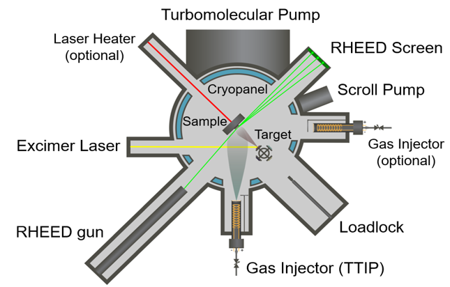
Top-down schematic view of the metal-organic pulsed laser deposition system. Red line is 808 nm diode laser for substrate heating. Yellow line is 248 nm excimer laser for laser ablation of the target material (SrO single crystal). Green line is 30 KeV electron beam for RHEED diffraction.
|
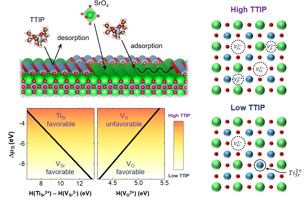
The metal organic precursor selectively adsorbs onto the Sr-terminated surface and not the Ti-terminated surface meaning a process window with 1:1 Ti:Sr stoichiometry is possible with this growth technique. In this growth window the point defect populations can be controlled.
|
|
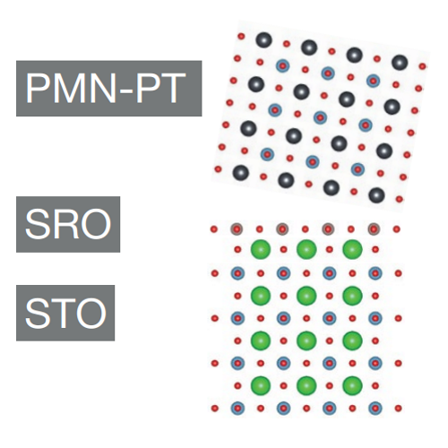
Magnetoelectric Coupling In Pb(Mg1/3Nb2/3)O3-PbTiO3 (PMN-PT) Membrane Heterostructures
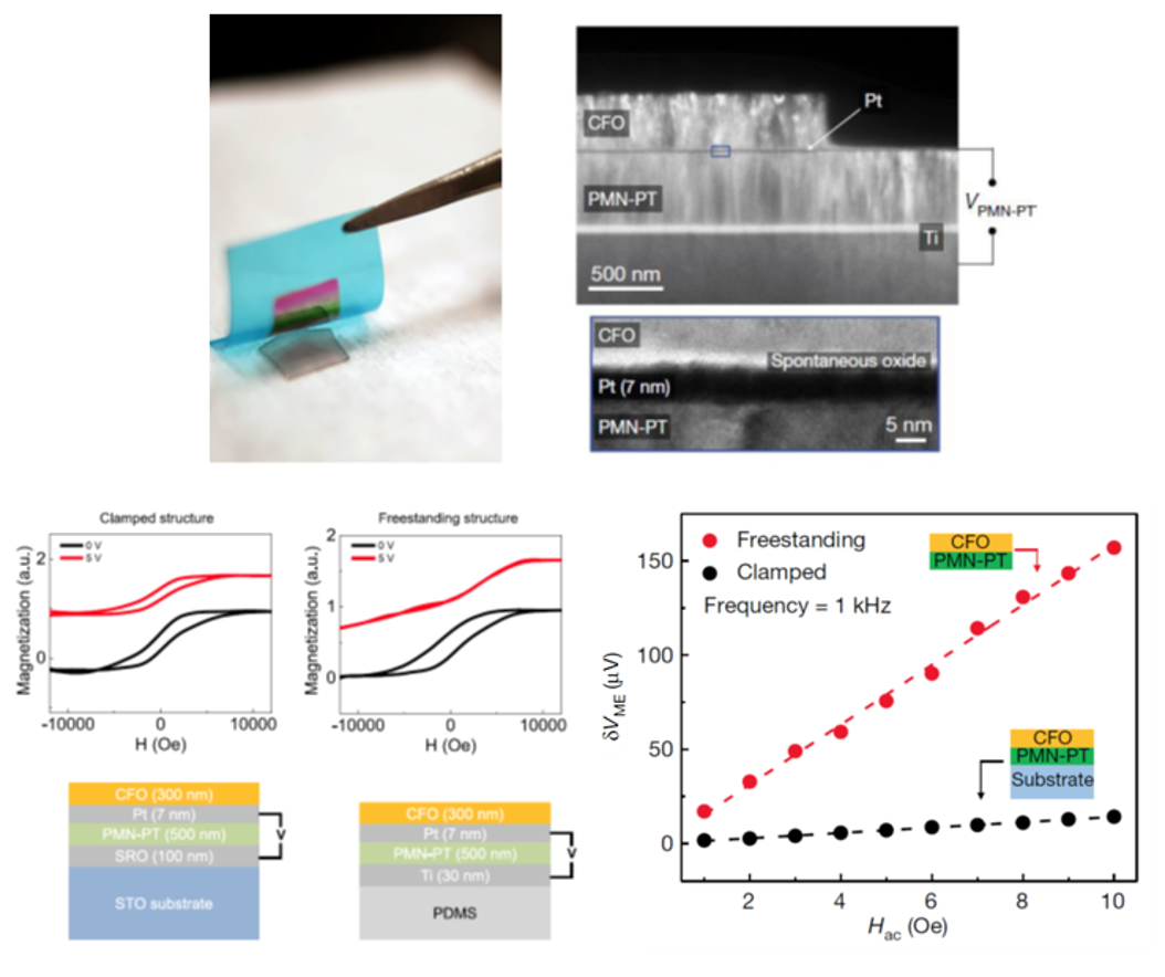
Exfoliation of epitaxial PMN-PT film from an SrTiO3 substrate (top left) frees it from the effect of substrate clamping. By coupling with a similarly-fabricated CoFe2O4 (CFO) (top right), the process of crystal stacking allows to create novel heterostructures that have been unachievable by conventional heteroepitaxy growth methods. Freed from the substrate clamping, the CFO/PMN-PT heterostructure shows an increase in strain-mediated magnetoelectric coupling. The bottom left shows the converse ME coupling between PMN-PT and CFO, while the bottom right demonstrates an increase in the direct ME coupling.
|
|
Relaxor-ferroelectrics like PMN-PT are well known for their giant piezoelectricity, i.e. the ability to generate large strains under application of an electric field (converse piezoelectric effect). Bulk single crystals show some of the largest piezoelectric coefficients of any known materials and find wide spread use as piezoelectric transducers in medical imaging, micro-positioners, and energy storage. However, by coupling with a magnetic material exhibiting large magnetostriction, the ferroelectric (FE) and ferromagnetic (FM) heterostructures can achieve enhanced functionality through the strain-mediated magnetoelectric (ME) coupling effect, where electric (magnetic) field control of magnetism (polarization) can lead to novel devices with applications in memory storage, magnetic/electric field sensing, and energy harvesting.
To realize such devices that meet the demands of high sensitivity and low power, thin films of both the FE and FM materials must be used. While bulk single crystals of PMN-PT show giant piezoelectricity (under application of ~100s V), thin films suffer from mechanical clamping by the passive substrate which reduces their piezoelectricity to almost zero. Therefore, the PMN-PT must be removed from its substrate, creating free-standing PMN-PT membranes, to achieve the giant piezoelectric effect once again (under application of ~1s V). Through a process of crystal stacking, we can create novel heterostructures that couple the PMN-PT with a variety of materials. By coupling with CoFe2O4 (CFO), we achieved large magnetoelectric coupling effects, including manipulation of the CFO’s magnetic anisotropy under application of only 5V. By applying this crystal stacking process to any materials, including complex oxides, 2-D materials, III-V’s, and many more, an unprecedented number of new combinations can lead to the discovery of novel physical phenomena, as well as the creation of innovative devices.
Kum, Hyun S., et al. "Heterogeneous integration of single-crystalline complex-oxide membranes." Nature 578.7793 (2020): 75-81.
|
|
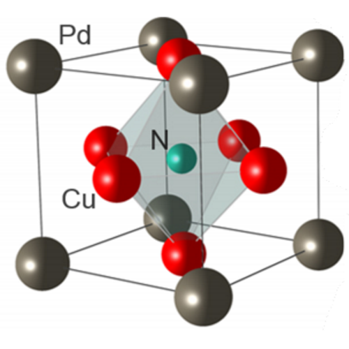
Epitaxial thin films of Dirac semimetal antiperovskite Cu3PdN
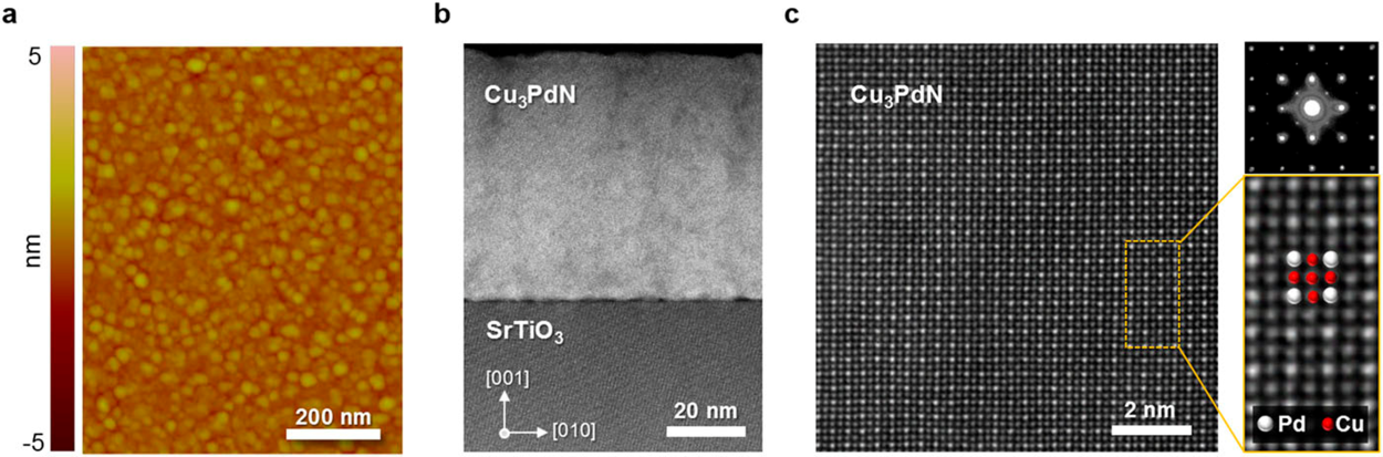
(a) Characteristic AFM image of Cu3PdN thin films. (b) Low magnification STEM image showing the Cu3PdN film and the top of the SrTiO3 substrate. (c) Atomic resolution STEM-HAADF image away from the interface. On the right, we show a selected area electron diffraction (SAED) pattern obtained in this region (top) and an enlarged region of the image including the [100] projected Cu3PdN unit cell (bottom).
|
|
The nitride antiperovskite Cu3PdN has been proposed as a new three-dimensional Dirac semimetal. However, the experimental realization of Cu3PdN and the consequent study of its electronic properties have been hindered due to the difficulty of synthesizing this material. We demonstrated the epitaxial Cu3PdN thin films grown on (001)-oriented SrTiO3 substrates by reactive magnetron sputtering and post-annealed in NH3 atmosphere, which is the vital first step to unlock its intrinsic physical properties. We showed that Cu3PdN is a metallic conductor, as predicted by theory, and that the magneto-transport properties depend on small variations in the nitrogen content. The nitrogen understoichiometry results in a decrease of the Fermi level below the Dirac node.
Quintela, C. X., et al. "Epitaxial thin films of Dirac semimetal antiperovskite Cu3PdN." APL Materials 5.9 (2017): 096103.
|
Spontaneous Hall effect enhanced by local Ir moments in epitaxial Pr2Ir2O7 thin films
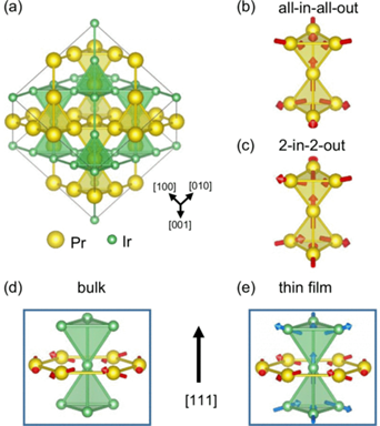
(a) Unit cell of Pr2Ir2O7 with only the cation sublattices shown. Oxygen atoms are not shown for clarity. (b), (c) “All-in–all-out” and “2-in–2-out” spin configurations on the Pr corner-sharing tetrahedra. (d), (e) Corner-sharing Ir tetrahedra surrounded by a Pr hexagonal ring in the (111) plane of the bulk and thin film, respectively. The red arrows in the Pr atoms indicate the Pr 4f moments. Due to the cubic symmetry breaking in the thin film, Ir local moments can be established indicated here in (e) by the blue arrows in the Ir atoms.
|
|
Rare-earth pyrochlore iridates (RE2Ir2O7) consist of two interpenetrating cation sublattices, the RE with highly frustrated magnetic moments, and the iridium with extended conduction orbitals significantly mixed by spin-orbit interactions. The coexistence and coupling of these two sublattices create a landscape for discovery and manipulation of quantum phenomena such as the topological Hall effect, massless conduction bands, and quantum criticality. Thin films allow extended control of the material system via symmetry-lowering effects such as strain. The Pr2Ir2O7 thin film was grown by solid phase epitaxy, a novel growth technique, where amorphous Pr2Ir2O7 was deposited on substrate via magnetron sputtering at room temperature with subsequent post annealing at high temperature. This novel growth technique broadens the growth condition of the composition including volatile species.
Guo, Lu, et al. "Spontaneous Hall effect enhanced by local Ir moments in epitaxial P r 2 I r 2 O 7 thin films." Physical Review B 101.10 (2020): 104405.
|
|
Superconductivity in undoped BaFe2As2 by tetrahedral geometry design
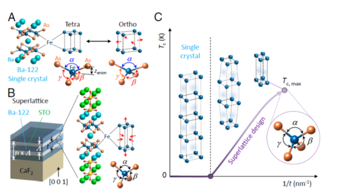
Emergent superconductivity in parent Ba-122 by superlattice design. (A) Fe sublattice and tetrahedral geometry in Ba-122 bulk single crystal below magnetostructural phase transition temperature. (B) Superlattice design for the control of Fe sublattice structure and FeAs4 tetrahedron in the presence of tetragonal-to-orthorhombic transition. (C) Emergent superconductivity by proximity to the regular tetrahedron via reduction of the Ba-122 layer thickness t in a Ba-122/SrTiO3 superlattice.
|
|
Fe-based superconductors exhibit a diverse interplay between charge, orbital, and magnetic ordering. Variations in atomic geometry affect electron hopping between Fe atoms and the Fermi surface topology, influencing magnetic frustration and the pairing strength through changes of orbital overlap and occupancies. Here, we experimentally demonstrate a systematic approach to realize superconductivity without chemical doping in BaFe2As2, employing geometric design within an epitaxial heterostructure. We control both tetragonality and orthorhombicity in BaFe2As2 through superlattice engineering, which we experimentally find to induce superconductivity when the As−Fe−As bond angle approaches that in a regular tetrahedron. This approach to superlattice design could lead to insights into lowdimensional superconductivity in Fe-based superconductors.
Kang, Jong-Hoon, et al. "Superconductivity in undoped BaFe2As2 by tetrahedral geometry design." Proceedings of the National Academy of Sciences 117.35 (2020): 21170-21174.
Kang, Jong-Hoon, et al. "Control of epitaxial BaFe2As2 atomic configurations with substrate surface terminations." Nano letters 18.10 (2018): 6347-6352.
|
|